- Hardware Manuals
- Commissioning and Tuning Guide
- Software Reference
- Resources
Important
One encoder has to be mounted on the motor side for commutation purpose. An encoder on a gear out side can not be used for commutation!
Note
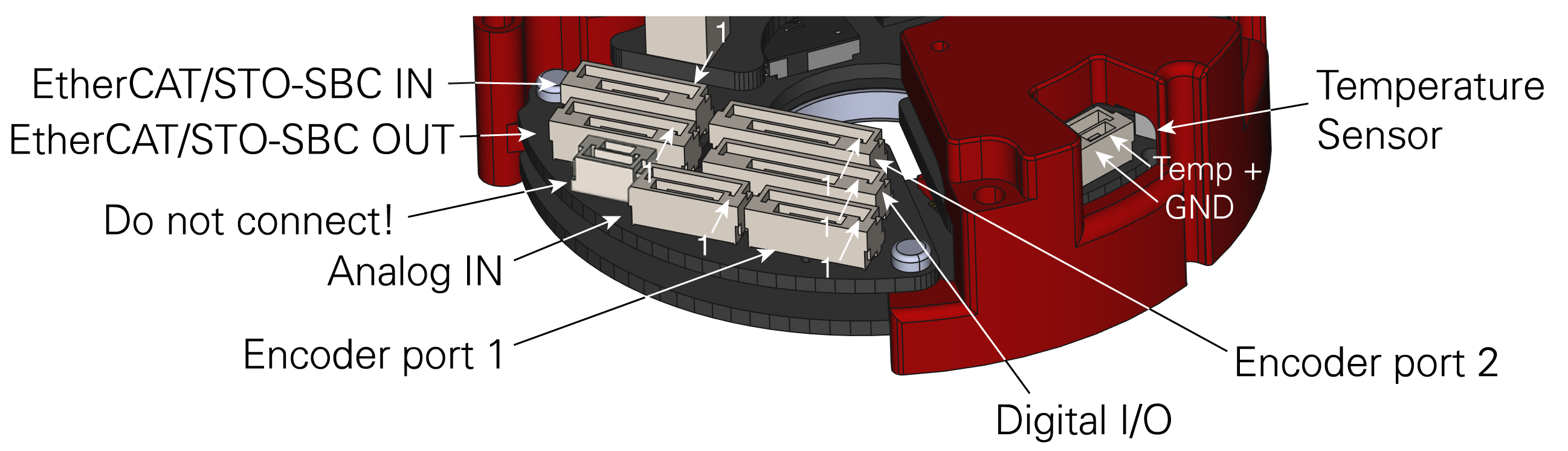
Details about measuring Analog signals can be found in our system integration guideline: Connecting and configuring analog inputs
Pin # |
Signal |
Function |
Object Mapping |
|---|---|---|---|
1 |
+5 V * |
Supply for external use ** |
|
2 |
Analog In 2 - |
Differential - |
Analog input 2 (0x2402) |
3 |
Analog In 2 + |
Differential + |
Analog input 2 (0x2402) |
4 |
GND |
Ground |
|
5 |
Analog In 1 |
Single-ended 0-5 V |
Analog input 1 (0x2401) |
6 |
not connected |
Note
Note
This connector also carries the pins for the battery that is required if the optional integrated encoder 1 is used with Multi-Turn. For selecting a suitable battery, please check these notes.
Protocol/Function |
Multi turn battery supply |
BiSS (Diff.) |
SSI (Diff.) |
|---|---|---|---|
Encoder Type |
Integrated Encoder 1 |
External Encoder on port 1 |
External Encoder on port 1 |
Pin # |
Config. # 1 |
Config. # 2 |
Config. # 3 |
1 |
5 V * |
||
2 |
MA- |
Clock- |
|
3 |
MA+ |
Clock+ |
|
4 |
Ground |
||
5 |
SLO- |
Data- |
|
6 |
SLO+ |
Data+ |
|
7 |
V_BAT |
||
* The current capacity of 5 V output is shared between all connectors and the total consumption is limited to 250 mA.
Pin # |
ABI / Fast ABI * (Diff.) |
ABI (Single-Ended) |
BiSS-C (Diff.) |
SSI (Diff.) |
Half-Duplex/A-Format (Diff.) |
HALL (Single-Ended) |
|---|---|---|---|---|---|---|
1 |
5 V ** |
|||||
2 |
MA- |
Clock- |
SD- / A |
|||
3 |
MA+ |
Clock+ |
SD+ / B |
|||
4 |
Ground |
|||||
5 |
A- |
A |
SLO- |
Data- |
H3 / C |
|
6 |
A+ |
SLO+ |
Data+ |
|||
7 |
B- |
B |
H2 / B |
|||
8 |
B+ |
|||||
9 |
I- |
I |
H1 / A |
|||
10 |
I+ |
|||||
* Fast ABI is supported from firmware 5.0 on
** The current capacity of 5 V output is shared between all connectors and the total consumption is limited to 250 mA.
Pin # |
GPIO |
REM 16MT |
BiSS(LVTTL) |
SSI (LVTTL) |
SPI |
|---|---|---|---|---|---|
1 |
+3.3 V OUT * |
||||
2 |
Digital I/O 1 (Fast Push-Pull) |
SCK |
SLO |
Data |
SCK |
3 |
Digital I/O 2 (Fast Push-Pull) |
MISO |
MA |
Clock |
MISO |
4 |
Ground |
||||
5 |
Digital I/O 3 (Fast Push-Pull) |
MOSI |
MOSI |
||
6 |
Digital Output 4 (Slow Push-Pull) ** |
SS |
SS |
||
7 |
+5 V OUT *** |
||||
8 |
Digital I/O 5 (Slow Bi-Directional) |
||||
9 |
Digital I/O 6 (Slow Bi-Directional) |
||||
10 |
Ground |
||||
11 |
Digital IN 7 (Slow 24 V) |
||||
Note
Note
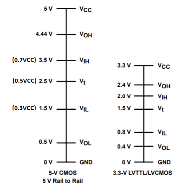
Voltage level |
3V3 (CMOS) |
5 V (CMOS) |
24 V (Only Digital In 7) |
|
|---|---|---|---|---|
Input |
V IH (min) |
2 V |
0.7 x Vcc |
16 V |
V IL (max) |
0.8 V |
0.3 x Vcc |
5 V |
|
Output |
V OH (min) |
2.4 V |
4.44 V |
|
V OL (max) |
0.4 V |
0.5 V |
||
Note
Pin # |
|
|---|---|
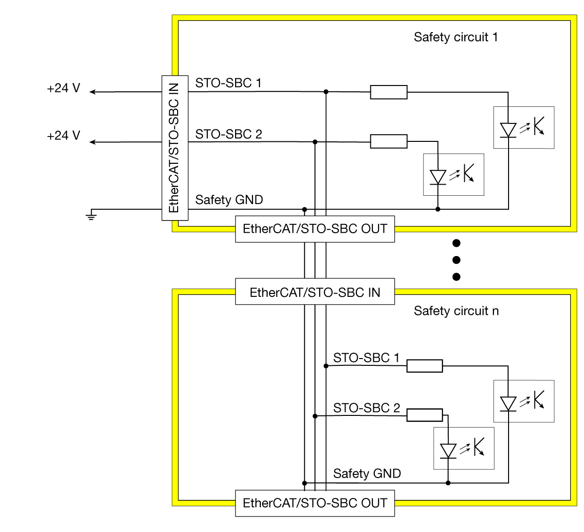
1 |
STO-SBC In 1 |
2 |
STO-SBC In 2 |
3 |
Safety GND |
4 |
RX_N |
5 |
RX_P |
6 |
TX_N |
7 |
TX_P |
8 |
FE |
Important
Please note that Safety GND is an isolated signal from drive GND.
Voltage level |
24 V logic Type 1 |
|---|---|
V IH |
15 V to 24 V |
V IL |
0 V to 5 V |
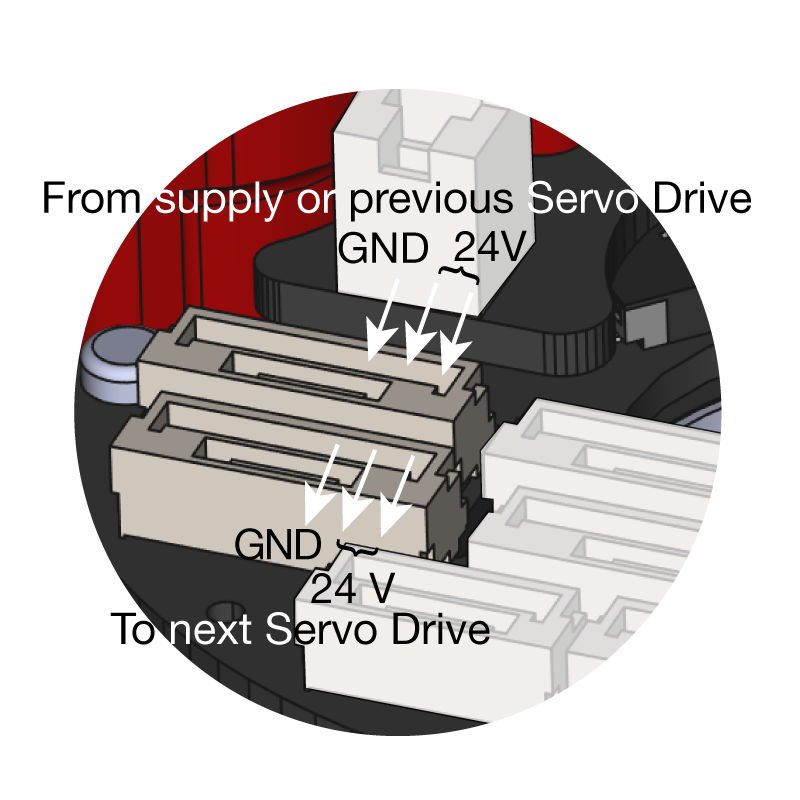
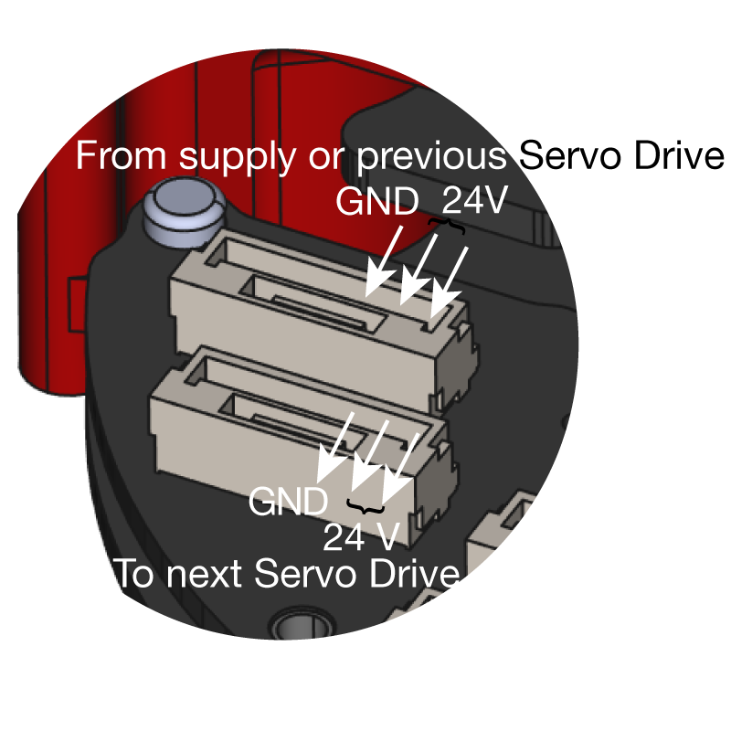
Attention
When not using the STO-SBC feature, please attach a +24 V supply to Pin 1 and 2 and Ground to Pin 3. It’s possible to daisy-chain these signals to other servo drives.