- Hardware Manuals
- Commissioning and Tuning Guide
- Software Reference
- Resources
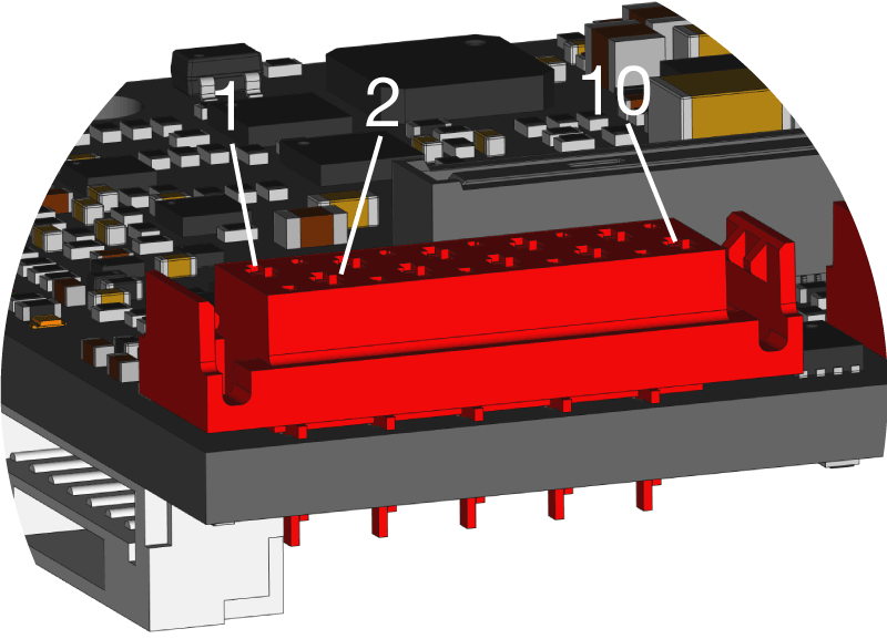
Pin # |
ABI * |
BiSS * |
SSI * |
Half-Duplex / A-Format * |
|---|---|---|---|---|
1 |
MA- |
Clock- |
SD- / A |
|
2 |
5 V ** |
5 V ** |
5 V ** |
5 V ** |
3 |
Ground |
Ground |
Ground |
Ground |
4 |
MA+ |
Clock+ |
SD+ / B |
|
5 |
A- |
SLO- |
Data- |
|
6 |
A+ |
SLO+ |
Data+ |
|
7 |
B- |
|||
8 |
B+ |
|||
9 |
I- |
|||
10 |
I+ |
Pin # |
HALL |
ABI (differential)* |
ABI (single-ended)** |
BiSS * |
SSI * |
|---|---|---|---|---|---|
1 |
MA- |
Clock- |
|||
2 |
5 V *** |
5 V *** |
5 V *** |
5 V *** |
5 V *** |
3 |
Ground |
Ground |
Ground |
Ground |
Ground |
4 |
MA+ |
Clock+ |
|||
5 |
C/H3 |
A- |
A |
SLO- |
Data- |
6 |
A+ |
SLO+ |
Data+ |
||
7 |
B/H2 |
B- |
B |
||
8 |
B+ |
||||
9 |
A/H1 |
I- |
I |
||
10 |
I+ |
Pin # |
GPIO |
REM 16MT |
BiSS (LVTTL) |
SSI (LVTTL) |
SPI |
Type of Port |
|---|---|---|---|---|---|---|
1 |
3.3 V * |
3.3 V * |
3.3 V * |
3.3 V * |
3.3 V * |
|
2 |
Digital IO 1** |
SS |
SLO |
Data |
SS/CS |
(Fast Push-Pull) |
3 |
Digital IO 2** |
SCK |
MA |
Clock |
SCK |
Fast port |
4 |
Ground |
Ground |
Ground |
Ground |
Ground |
|
5 |
Digital IO 3** |
MISO |
MISO |
Fast port |
||
6 |
Digital IO 4** |
MOSI |
MOSI |
Fast port |
||
7 |
5 V *** |
5 V *** |
5 V *** |
5 V *** |
5 V *** |
|
8 |
Note
Note
Details about measuring Analog signals can be found in our system integration guideline: Connecting and configuring analog inputs
Pin # |
Default Setting * |
Object Mapping |
|
|---|---|---|---|
1 |
|||
2 |
Analog Input 1 - |
Connect to Ground ** |
|
3 |
Analog Input 1 + |
Single-ended 0-10 V |
Analog input 1 (0x2401) |
4 |
Ground |
||
5 |
Analog Input 2 - |
Connect to Ground ** |
|
6 |
Analog Input 2 + |
Single-ended 0-10 V |
Analog input 2 (0x2402) |
7 |
5 V *** |
||
8 |
10 V **** |
||
9 |
Analog Input 3 - |
Differential ±5 V |
Analog input 3 (0x2403) |
10 |
Analog Input 3 + |
Differential ±5 V |
Analog input 3 (0x2403) |
11 |
Analog Input 4 - |
Differential ±5 V |
Analog input 4 (0x2404) |
12 |
Analog Input 4 + |
Differential ±5 V |
Analog input 4 (0x2404) |
Symbol |
Min. |
typical |
Max. |
Description |
Impact |
|---|---|---|---|---|---|
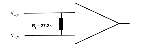
V diff |
-10V |
+10V |
The input voltage between the positive and negative input pins. |
Any voltage out of this range causes saturation to min/max ADC value |
|
V cm |
-10V |
0V |
+10V |
The common mode voltage. |
Any voltage out of this range causes saturation and inaccuracy in the measurements. |
V in,P |
-15V |
+15V |
The tolerable voltage between the positive input pin and GND. |
Any voltage out of this range damages the analog input’s circuitry. |
|
V in,N |
-15V |
+15V |
The tolerable voltage between the negative input pin and GND. |
Any voltage out of this range damages the analog input’s circuitry. |
|
R i |
27.2kΩ |
Internal input resistance |
|||
Error |
-1% |
+1% |
Error in ticks |
Symbol |
Min. |
typical |
Max. |
Description |
Impact |
|---|---|---|---|---|---|
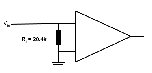
V :sub`in` |
0V |
+1V |
The input voltage between the input and GND. |
Any voltage out of this range causes saturation to min/max ADC value |
|
V in,lim |
-15V |
+15V |
The tolerable input voltage between the input and GND. |
Any voltage out of this range damages the analog input’s circuitry. |
|
R i |
20.4kΩ |
Internal input resistance |
|||
Error |
-1% |
+1% |
Error in ticks |
There is no particular input for temperature sensors in Node. Four analog inputs are available. Any of these can be used to measure the temperature sensor resistance. But the single-ended (AI 1, AI 2) is more accurate than the differential inputs (AI 3, AI 4) because the voltage difference is less. A simple circuit with an extra resistor for voltage dividing has to be implemented externally. For details about using temperature sensors please check our System integration guide.
A voltage divider is needed when the Analog In needs to be calibrated. This is required for adjusting the measuring range when using a temperature sensor.
The image below depicts how to connect an RTD sensor resistance using the single-ended analog input.
Attention
The ADC value is scaled to 16 bit since firmware v5.0.
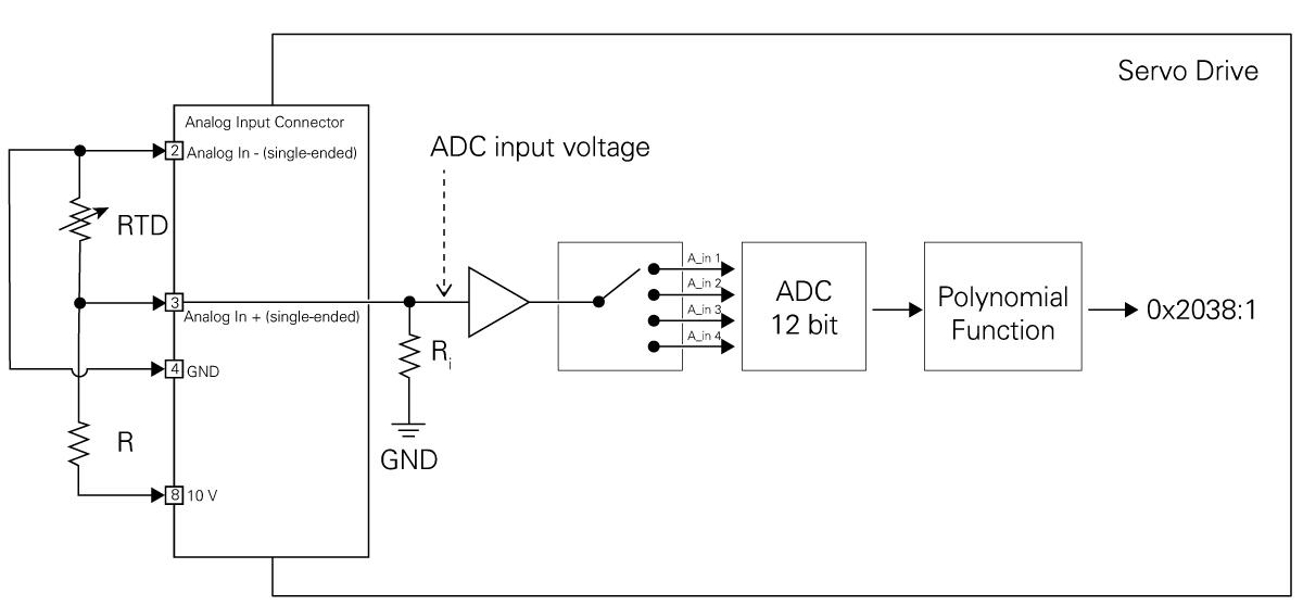
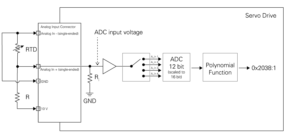
The internal resistance R i of the single-ended analog input is 20.4 kΩ and it is connected in parallel to the RTD sensor.
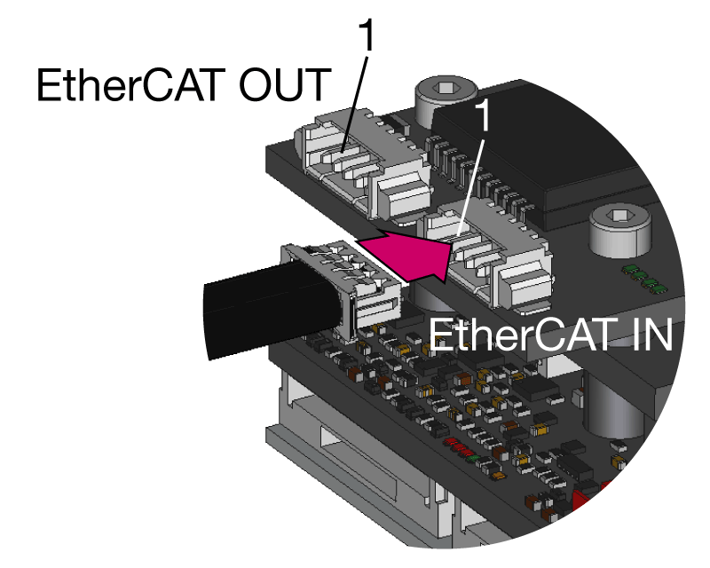
Pin |
Name |
Function |
|---|---|---|
1 * |
TX+ |
Differential transmit pair, positive line |
2 |
TX- |
Differential transmit pair, negative line |
3 |
Shield |
|
4 |
RX+ |
Differential receive pair, positive line |
5 |
RX- |
Differential receive pair, negative line |
* Pin 1 is on left
Pin |
Name |
Function |
|---|---|---|
1 * |
TX+ |
Differential transmit pair, positive line |
2 |
TX- |
Differential transmit pair, negative line |
3 |
Shield |
|
4 |
RX+ |
Differential receive pair, positive line |
5 |
RX- |
Differential receive pair, negative line |
* Pin 1 is on left
