- Hardware Manuals
- Commissioning and Tuning Guide
- Software Reference
- Resources
This feature allows using the Digital Inputs of the Drive to command actions and to configure the Digital Outputs to trigger when certain events happen. This can be used to control some aspects of the Drive with an external signal or to control an external device with the Drive.
Available features are:
0 Disabled (default)
2 [IN] General Purpose Input
3 [OUT] General Purpose Output
4 [IN] Home Switch Active High - Level Triggered
5 [IN] Home Switch Active Low - Level Triggered
6 [IN] Positive Limit Switch Active High - Level Triggered for Homing & Edge Triggered (Latch) for Error (PosLmAct)
7 [IN] Positive Limit Switch Active Low - Level Triggered for Homing & Edge Triggered (Latch) for Error (PosLmAct)
8 [IN] Negative Limit Switch Active High - Level Triggered for Homing & Edge Triggered (Latch) for Error (NegLmAct)
9 [IN] Negative Limit Switch Active Low - Level Triggered for Homing & Edge Triggered (Latch) for Error (NegLmAct)
10 [IN] Interlock (Disable Operation) Active Low - Level Triggered
11 [IN] Fault Reset - Edge Triggered
12 [IN] Interlock (Fault Reaction) Active Low - Level Triggered
13 [IN] Time Stamped Rising Edge - Edge Triggered
14 [OUT] Mimics Target Reached (tr) Bit of Statusword
15 [OUT] Mimics Internal Limit Active (ila) Bit of Statusword
16 [OUT] Timestamped Triggered Output
17 [OUT] Position Triggered Output (Pulse)
18 [OUT] Mimics Fault (f) Bit of Statusword
19 [OUT] Mimics Switched On (so) Bit of Statusword
20 [OUT] Mimics Ready to Switch On (rtso) Bit of Statusword
21 [OUT] Mimics Operation Enabled (oe) Bit of Statusword
22 [OUT] Mimics Voltage Enabled (ve) Bit of Statusword
23 [OUT] Mimics Switch On Disabled (sod) Bit of Statusword
24 [OUT] Mimics Quick Stop (qs) Bit of Statusword
25 [OUT] Mimics Warning (w) Bit of Statusword
You can access the features in OBLAC Drives: Enter Feedback & IO/Digital IO
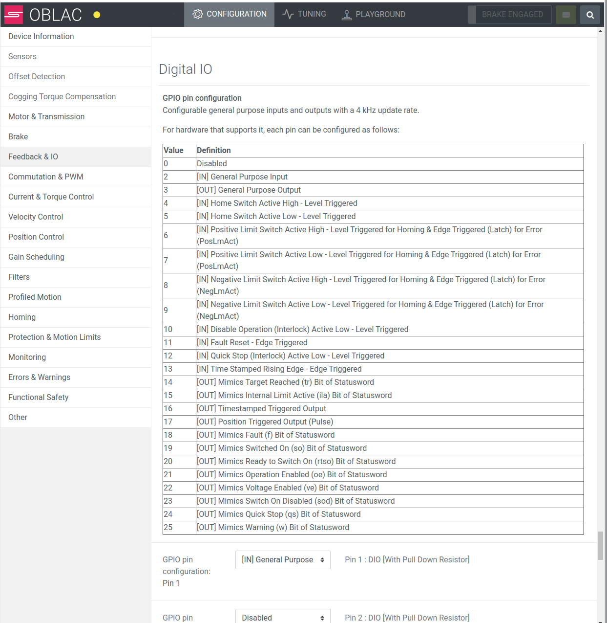
The actions and events on GPIO pins can also be configured manually in object Object 0x2210 (GPIO Pin Configuration).
In this object a feature can be selected for each Digital I/O pin.
Some features require additional settings in other objects as well.
Attention
Ensure that the selected pin allows the direction of the feature:
Attention
Each feature can only be used on one pin (except for General Purpose Input and General Purpose Output)
General Purpose Input (2)
The high and low logic (voltage levels) at the selected GPIO pin will be reflected in the corresponding bits of object 0x60FD (Digital Inputs) as 1 and 0 respectively.
General Purpose Output (3)
The value of the selected digital output is high if the corresponding bit in sub-object 0x60FE:1 is high and the corresponding mask bit in sub-object 0x60FE:2 is set as 1.
The output value will be the value set in the object 0x60FE:1 (Digital Output).
Note
Limit switch and Home switch configuration are used when the drive is in Homing Mode. Limit switches can also trigger Quick Stop in all modes. In homing mode Quick Stop is triggered by the limit switch if it is not being used by the homing method.
Home Switch Active High - Level Triggered (4)
Active and inactive state of the Home switch will be reflected as 1 and 0 respectively at the selected digital input.
Home Switch Active Low - Level Triggered (5)
Active and inactive state of the Home switch will be reflected as 0 and 1 respectively at the selected digital input.
Note
Irrespective of the switch type (Active High or Active Low), active and inactive states of the home switch will be shown as 1 and 0 respectively in bit 2 (home switch) of the Digital Input Object 0x60FD.
Positive Limit Switch Active High - Level Triggered for Homing & Edge Triggered (Latch) for Error (PosLmAct) (6)
Active and inactive state of the Positive limit switch will be reflected as 1 and 0 respectively at the selected digital input.
Positive Limit Switch Active Low - Level Triggered for Homing & Edge Triggered (Latch) for Error (PosLmAct) (7)
Active and inactive state of the Positive limit switch will be reflected as 0 and 1 respectively at the selected digital input.
Note
Irrespective of the switch type (Active High or Active Low), active and inactive states of the positive limit switch will be shown as 1 and 0 respectively in bit 1 (positive limit switch) of the Digital Input Object 0x60FD.
Note
Positive Limit switch also triggers Quick Stop, if the drive is either in any opmode other than HOMING or the drive in is HOMING mode but the switch is not being used by the homing method. If Positive Limit Switch has been activated in this case, then bit 2 (qs) of the Controlword will be cleared and Quick Stop will be executed.
Negative Limit Switch Active High - Level Triggered for Homing & Edge Triggered (Latch) for Error (NegLmAct) (8)
Active and inactive state of the Negative limit switch will be reflected as 1 and 0 , in the corresponding bit (according to configured GPIO) of the object 0x60FD (Digital Inputs)
Negative Limit Switch Active Low - Level Triggered for Homing & Edge Triggered (Latch) for Error (NegLmAct) (9)
Active and inactive state of the Negative limit switch will be reflected as 0 and 1 , in the corresponding bit (according to configured GPIO) of the object 0x60FD (Digital Inputs)
Note
Irrespective of the switch type (Active High or Active Low) , active and inactive states of the negative limit switch will be shown as 1 and 0 respectively in bit 0 (negative limit switch) of the Digital Input Object 0x60FD.
Note
Negative Limit switch also triggers Quick Stop, If drive is either in any opmode other than HOMING or drive in is HOMING mode but the switch is not being used by the homing method. If Negative Limit Switch has been activated in this case, then bit 2 (qs) of the Controlword will be cleared and Quick Stop will be executed.
Driving out of the limit switch is only possible in the opposite direction, the concrete behavior is mode-dependant:
Modes CSP, PP , PV , CSV , CST and PT
If a target is commanded which would move the axis further into the direction of the switch, the motor will stand still, since further movement in the direction of switch is not allowed.
Cogging torque compensation
If the switch is active and the user tries to switch to cogging torque compensation, this will not be allowed.
The error based on the activated switch will be raised by firmware.
Diagnostics mode
The following OS commands are not executed, if either of the limit switches is active:
OS command 2 (Open Loop Field Mode)
OS command 4 (Motor Phase Order Detection)
OS command 5 (Commutation offset detection with Methods 0 and 1)
OS command 6 (Open phase detection)
OS command 7 (Pole pair detection)
OS command 8 (Phase Resistance Measurement)
OS command 9 (Phase Inductance Measurement)
If any of these OS commands is called while a limit switch is active, the response will be OSCMD_ERROR_CMD_NOT_ALLOWED.
The following OS commands can be executed, even if either of the limit switches is active:
OS command 0 (Encoder register communication)
OS command 1 (iC-MU calibration mode)
OS command 3 (HRD streaming)
OS command 5 (Commutation offset detection with Method 2)
Homing modes
If the switch is active then Homing is only allowed in those modes that will take the axis away from the activated switch. All those methods which try to move the axis further into the limit switch will raise an error.
The error raised depends on the limit switch being active:
For a positive limit switch the error raised will be PosLmAct
For a negative limit switch the error raised will be NegLmAct
Use case: Interlock
When connecting different devices for a common process it’s often necessary to ensure the correct order of operation. This can be done by routing the signals to the master but it comes at a cost for reaction-time, data load and additional wiring. Input actions allow interlocking an operation directly at the Drive to guarantee the correct order of the process.
Interlock (Disable Operation) Active Low - Level Triggered (10)
Clear bit 3 (eo) of controlword when the selected digital input is low.
This will cause the drive to transition into Operation disable state.
Interlock will remain active as long as the configured GPIO remains low and transitioning into OP Enabled state will not be possible. Transitioning into OP Enabled state will only be possible when interlock is deactivated by setting the GPIO input high. Bit 3 (interlock bit) of the Digital Inputs Object 60FD will also be high when Interlock is active.
Fault reset (11)
Set bit 7 (fr) of controlword when the selected digital input is high.
Interlock (Fault Reaction) Active Low - Level Triggered (12)
Raises the fault “Interlck”, when the selected digital input is low.
This will cause the drive to transition into Fault Reaction State.
Interlock will remain active as long as the configured GPIO remains low and entering into OP Enabled state will not be possible. If OP Enabled state is attempted to be entered while interlock is active, Interlck fault will be raised again by the firmware. Transitioning into OP Enabled state will be possible when interlock is deactivated by setting the configured GPIO input high. Bit 3 (interlock bit) of the Digital Inputs Object 60FD will also be high when Interlock is active.
Time Stamped Rising Edge - Edge Triggered (13)
Report a rising edge timestamp with 2 µs accuracy if GPIO is a fast port (as indicated in the table below). Otherwise the accuracy is 62.5 µs. The value of this GPIO is updated in shared memory at 16 kHz.
Mimics Target Reached (tr) Bit of Statusword (14)
The value of the selected Digital Output mimics bit 10 of the Statusword (tr). When the “tr” bit is high, the configured digital output will be high
Mimics Internal Limit Active (ila) Bit of Statusword (15)
The value of the selected Digital Output mimics bit 11 of the Statusword (ila). When the “ila” bit is high, the digital output value will be high.
Timestamp triggered Output (16)
Trigger the Digital Output at a certain timestamp. The output value will be the value set in the object 0x60FE:1 (Digital Output).
The value specified in subitem 1 of object 0x2211 (GPIO output events) is the Timestamp at which the GPIO should trigger. The unit is in 10 ns.
The value in 0x2211:1 can be used for setting this timestamp. But the unit must be converted to 10 of ns.
Note
The value need to be converted to be in the same time reference (1 µs vs. 10 ns)
Example:
The value read in object 0x20F0:0 is 2385309 µs. The Timestamp triggered output shall be triggered 15000 µs after the current time. Both times need to be converted to the units of 0x2211:1 and added: 2385309 * 100 + 15000 * 100 = 240030900.
Attention
When the DC Clock feature is not used, there is a drift between the timestamp and the DC Clock.
Note
If the GPIO is a fast port, this is activated with an accuracy of 10 ns. Otherwise the accuracy is 62.5 µs.
Please refer to the table below for the type of port:
SOMANET Circulo |
SOMANET Node |
|
|---|---|---|
Digital I/O 1 |
Fast port |
Fast port |
Digital I/O 2 |
Fast port |
Fast port |
Digital I/O 3 |
Fast port |
Fast port |
Digital Output 4 |
Slow port |
N/A |
Digital I/O 4 |
N/A |
Fast port |
Digital I/O 5 |
Slow port |
N/A |
Digital I/O 6 |
Slow port |
N/A |
Digital Input 7 |
Slow port |
N/A |
Position Triggered Output (Pulse) (17)
Output a configurable width pulse to the selected Digital Output at a certain encoder position. The encoder port that is used can be selected in subitem 2 of object 0x2213:
SOMANET Circulo |
SOMANET Node |
|
|---|---|---|
Encoder Connector 1 |
Internal encoder 1 |
Encoder Port 1 |
Encoder Connector 2 |
Internal encoder 2 |
Encoder Port 2 |
Encoder Connector 3 |
Encoder port 1 |
Encoder Port 3 / Digital IO |
Encoder Connector 4 |
Encoder port 2 |
|
Encoder Connector 5 |
Digital I/O |
Note
If an ABI encoder is used,the response will be almost immediate (within 0.34 µs). If another encoder type is selected, the response will be slower (within 62.5 µs).
Object 0x2213 allows further configuration of this output event by setting the following parameters:
Pulse Width
Position Setpoint at which the pulse needs to occur at GPIO
Selection of the encoder for which setpoint is defined.
Mimics Fault (f) Bit of Statusword (18)
The value of the selected Digital Output mimics bit 3 of the Statusword (f). When the “f” bit is high, the selected digital output will be high.
Mimics Switched On (so) Bit of Statusword (19)
The value of the selected Digital Output mimics bit 1 of the Statusword (so). When the “so” bit is high, the selected digital output will be high.
Mimics Ready to Switch On (rtso) Bit of Statusword (20)
The value of the selected Digital Output mimics bit 0 of the Statusword (rtso). When the “rtso” bit is high, the selected digital output will be high.
Mimics Operation Enabled (oe) Bit of Statusword (21)
The value of the selected Digital Output mimics bit 2 of the Statusword (oe). When the “oe” bit is high, the selected digital output will be high.
Mimics Voltage Enabled (ve) Bit of Statusword (22)
The value of the selected Digital Output mimics bit 4 of the Statusword (ve). When the “ve” bit is high, the selected digital output will be high.
Mimics Switch On Disabled (sod) Bit of Statusword (23)
The value of the selected Digital Output mimics bit 6 of the Statusword (sod). When the “sod” bit is high, the selected digital output will be high.
Mimics Quick Stop (qs) Bit of Statusword (24)
The value of the selected Digital Output mimics bit 5 of the Statusword (qs). When the “qs” bit is high, the selected digital output will be high.
Mimics Warning (w) Bit of Statusword (25)
The value of the selected Digital Output mimics bit 7 of the Statusword (w). When the “w” bit is high, the selected digital output will be high.
Timestamp at which the GPIO should trigger for “Timestamped Triggered Output”
Time of the last rising edge for “Timestamped Rising Edge”
Sets Pulse Width, Position Setpoint and the encoder for “Position Triggered Output”
Note
The pulse is generated independantly of the direction from which the setpoint is crossed.
Manufacture specific bits set the state of digital output
Manufacture specific bits show the state of digital inputs.
